ALCF simulations shed light on technique to alter materials properties
Alchemy has long been perceived as the practice of transmuting base metals, like iron and lead, into gold, through a conflation of chemical and mystical methodologies. Though considered a pseudoscience, it drew to it some key figures in chemistry and physics, and supported the early Greek philosophical construct that all matter was comprised of invisible particles that acted upon one another.
Today, we know those particles as atoms and their subatomic constituents. And despite their more mystical aspirations, alchemists did indeed achieve scientific breakthroughs in chemistry and metallurgy, among other areas, likely through chance manipulations of key molecules and atoms.
Several centuries after alchemy’s apex, Aiichiro Nakano and a multi-institutional research team led by the University of Southern California (USC) are taking a more modern approach to exploring the nature of invisible particles for the purpose of transmutation.
In doing so, they have replaced the crucible and furnace of the alchemist’s solitary laboratory with much more powerful tools; the computational and accelerator power of two U.S. Department of Energy (DOE) Office of Science laboratories, Argonne National Laboratory and SLAC National Accelerator Laboratory, respectively.
Nakano, a professor of computer science at USC, with joint appointments in physics, materials science and biology, is using the resources of the Argonne Leadership Computing Facility (ALCF), a DOE Office of Science User Facility, to observe how changes in the atomic structure of a semiconductor material might convert it to metal.
The ability to do so could drastically reduce the time and cost required to manufacture semiconductors—key components in most electronic devices—and extend their use to more novel applications, like flexible electronics.
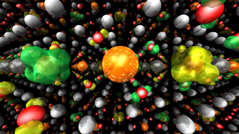
Last year, the team reported on its efforts in a Nature Communications paper describing the design of a multi-layered semiconductor constructed of two atomically thin layers of selenium sandwiching a layer of molybdenum, otherwise called molybdenum diselenide (MoSe2).
“This 2D material is very thin,” notes Nakano. “If you want to read information from this device, you need to insert metal leads, like aluminum or gold, but this turns out to be very bulky. So, what we are trying to do is basically convert semiconductor materials into metal by shining light on it.”
In an experiment designed to understand how this works, their SLAC collaborators used a high-brightness, ultrafast electron beam delivered through a unique experimental technique developed at SLAC, called mega-electron-volt Ultrafast Electron Diffraction. Short pulse durations and wavelengths allow the beam to probe these atomically thin materials at relevant spatiotemporal scales, providing a more accurate portrait of the relationship between structure and dynamics.
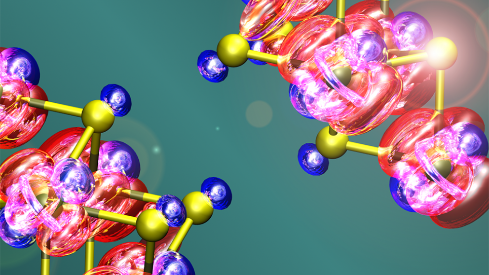
Shining laser light on the MoSe2 semiconductor creates a slight sliding of the top layer with respect to the middle and bottom layers. This minute shift changes the relative position of the atoms, thus changing the material’s properties and producing something completely different — in this case, a metallic version of MoSe2.
To better understand the physical mechanism underlying this reaction, Nakano’s team ran nonadiabatic quantum molecular dynamics (NAQMD) simulations on the ALCF’s Mira supercomputer. ALCF staff members assisted the team with performance profiling and tuning of NAQMD at scale on Mira, and helped with the visualization and analysis of the large simulation datasets generated on the system.
Molecular dynamics follows the movement of atoms as a function of time. Quantum molecular dynamics simulations allowed researchers to replicate the ultrafast — subpicosecond, or trillionth of a second — increase in lattice temperatures observed in SLAC experiments and the subsequent conversion of electronic energy from the laser light to the movement of atoms in the semiconductor’s top layer.
More importantly, NAQMD simulations were able to show that this conversion is caused by “softening” of vibrational modes in the excited state.
Before being disturbed by the laser light, atoms in the lattice are at rest “in a most comfortable position,” says Nakano. So trying to displace them to create a specific structural change takes no random act, as their spring-like constitution always returns them to that comfortable position.
To make the process work, the atoms must be seated in an alternate lattice position where they are equally comfortable. The light interacts with electrons in such a way as to break that spring-like hold in a process called phonon softening. This allows the atoms to move into a new position, potentially transforming the electronic property of the material from semiconducting to metal.
“We have been doing this kind of simulation for some years, but I never imagined in my lifetime that the experimentalists would be able to see the phenomena on the same time scale and the spatial scale. It’s so tiny and it occurs so fast,” exclaims Nakano.
So far, research results have been varied, but promising.
The work showed that nearly 100 percent of the laser light’s electronic excitation energy was transferred to atoms in the semiconductor, without losing energy to heat dissipation.
“That was not trivial, that was good news,” says Nakano. “All the energy from the laser light went into the motion of the atoms.”
Although the efficiency exceeded expectations, the displacement of the atoms achieved experimentally at SLAC was not enough to convert the semiconductor to metal. Nakano’s team continues to conduct further simulations on new and altered materials, like rhenium-augmented MoSe2, to determine the exact composition necessary to achieve the transition.
“We are testing many other materials in the hope that the light-induced atomic motion produced is greater than what we have achieved, so far. The Nature Communications paper showed proof of concept, proof that a phase transition from semiconductor to metal is possible,” says Nakano.
This work was supported as part of the Computational Materials Sciences Program funded by the DOE Office of Science, Basic Energy Sciences Program. ALCF computing time and resources were awarded through DOE's Innovative and Novel Computational Impact on Theory and Experiment (INCITE) program.
Argonne National Laboratory seeks solutions to pressing national problems in science and technology. The nation's first national laboratory, Argonne conducts leading-edge basic and applied scientific research in virtually every scientific discipline. Argonne researchers work closely with researchers from hundreds of companies, universities, and federal, state and municipal agencies to help them solve their specific problems, advance America's scientific leadership and prepare the nation for a better future. With employees from more than 60 nations, Argonne is managed by UChicago Argonne, LLC for the U.S. Department of Energy's Office of Science.
The U.S. Department of Energy's Office of Science is the single largest supporter of basic research in the physical sciences in the United States and is working to address some of the most pressing challenges of our time. For more information, visit the Office of Science website.
Domains
Allocations