Boosting Beamline Performance
Recent work by a collaboration of Advanced Photon Source (APS) beamline scientists and computer scientists at the Argonne Leadership Computing Facility (ALCF) and Mathematics and Computer Science (MCS) Division has produced breakthroughs in computational methods and infrastructure that boost beamline performance significantly.
High-energy X-ray beams at Argonne’s Advanced Photon Source, a U.S. Department of Energy (DOE) Office of Science User Facility, can be used to peer inside structures at the atomic level, making them especially useful for scientists designing next-generation materials for everything from computer memory chips to airplane components.
The APS generates the “brightest” high-energy synchrotron X-rays in the Western Hemisphere, a billion times more powerful than an X-ray tube, which are organized into individual beamlines for experimental use and optimized for particular types of investigations.
Hemant Sharma, a General Electric Company (GE)-funded postdoc, and APS physicist Jonathan Almer are developing new experimental techniques and algorithms at the 1-ID beamline to image the grain structures of polycrystalline materials—solid materials, like metals and ceramics, that are composed of variously sized and oriented microscopic crystals, called crystallites. One such technique, called high-energy diffraction microscopy (HEDM), can determine the grain-level properties of these materials across a range of applied thermal and mechanical loading conditions.
Sharma’s research includes testing metal samples supplied by GE, a major jet engine manufacturer, to determine their grain structure and defects. The methodology developed is quite general, however, and can be applied to other applications including energy (wind turbines) and transportation (automobile bodies).
Researchers working at the APS build and run entire experiments in a matter of days, storing and later retrieving the experimental data for analysis. Time on a beamline (‘beamtime’) is a precious commodity: beamline science teams are expected to staff their experiments 24 hours a day. If any part of the experimental setup is done incorrectly, it may be several months before they have an opportunity to try again.
Sharma’s experiment received a three-day allocation of Sector 1-ID beamtime last August. Mounting the sample in the radiation-shielding enclosure containing the beamline elements, the hutch, may consume as much as the entire first day due to the extensive instrumentation involved.
The beamline hutch is equipped with remote-controlled stages and cameras that work in concert to slowly rotate and take hundreds of thousands of snapshots, ultimately producing a 3D image and many gigabytes of data in the process. Using a video feed and control interfaces, Sharma set up the experimental parameters to calibrate the detectors and move the sample within the beam. To yield useful data, the positioning of the detector must to be accurate and stable within tens of microns.
The HEDM technique Sharma uses can be performed in two different ways: near-field (NF), with the detector extremely close to the sample, and far-field (FF), with the detector placed up to a meter or more away. NF-HEDM and FF-HEDM can be used together to obtain a higher-fidelity study of a given sample. This multi-modal approach can determine local strains that lead to cracks, enable microstructure-sensitive modeling, and validate additive manufacturing processes. However, until recently, HEDM has been severely limited by the enormous complexity and computational costs of the post-processing, reconstruction, and analysis process by which the captured 2D data is turned into a usable 3D grain images.
A solution to a big data, big compute problem
Sharma reserved eight racks of Mira, the IBM Blue Gene/Q supercomputer at the Argonne Leadership Computing Facility, also a DOE Office of Science User Facility, which gave him access to 131,072 compute cores to run an analysis job on the NF segment of his experimental procedure on days two and three of his beamtime.
To make the most of the machine’s power, Sharma worked with MCS computer scientist Justin Wozniak to use the Swift parallel scripting language to transform the HEDM analysis software into a scalable application capable of utilizing Mira efficiently. With Swift, users can write simple scripts that run many invocations of ordinary programs concurrently as soon as their inputs are available. Swift applications consisting of billions of program invocations, thousands at a time, run on everything from a PC to a cloud to a supercomputer.
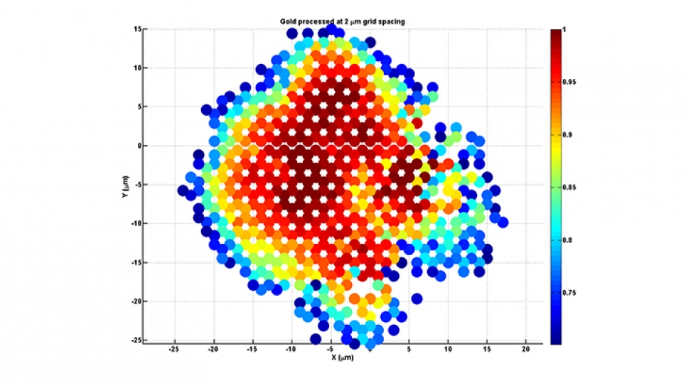
Sharma processed the first several layers of images, each composed of hundreds of thousands of images, in a few minutes on Mira. The resulting images showed obviously skewed data. Sharma adjusted the experimental hardware and took new trial images until the confidence levels indicated a correct physical setup. The culprit: a cable was too short, constraining the detector’s movement.
Without such in-beam experiment and computational assessment, said Sharma, the two-day session would have proceeded to completion, yielding useless data that would be discovered weeks or months later during a manual data analysis phase. By using Mira to help detect and correct a problem early on, Sharma’s two-day experiment instead produced publishable results.
The work was funded by General Electric; the U.S. Department of Energy, Office of Science, Office of Basic Energy Sciences; the U.S. Department of Energy, Office of Science, Office of Advanced Scientific Computing Research; and the U.S. National Science Foundation.
Argonne National Laboratory is supported by the Office of Science of the U.S. Department of Energy. The Office of Science is the single largest supporter of basic research in the physical sciences in the United States, and is working to address some of the most pressing challenges of our time. For more information, please visit science.energy.gov.