Credit: Shutterstock
Credit: Shutterstock
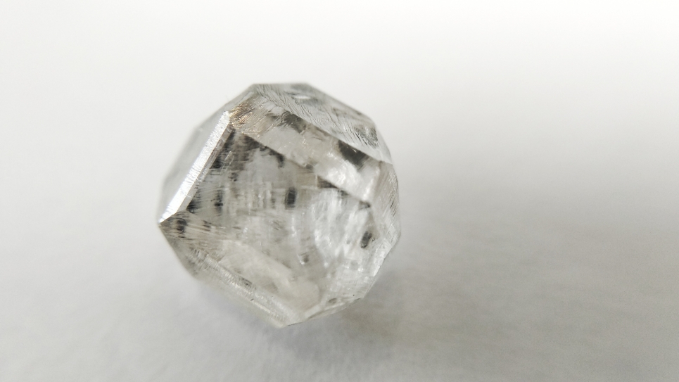
Abstract: Diamond is a semiconductor with extreme and unique properties, which enable applications for high power, high temperature electronics, radiation detectors, and electron emitters for ultra-high voltage vacuum switches and traveling wave tube cathodes. The fundamental structure for each of these applications is the p-i-n diode prepared from epitaxial, doped diamond layers. The availability of high-quality diamond substrates and the development of plasma CVD of epitaxial doped and undoped diamond have enabled fabrication of diodes with high breakdown field. CVD growth of high purity intrinsic diamond has shown room temperature mobility of both electrons and holes > 5000 cm2/V-s. Boron and Phosphorus doped layers achieve p-type and n-type character, respectively. Highly doped layers > 1019 cm-3 demonstrate low resistance through hopping conduction, which supports low resistance contacts. Epitaxial diamond PIN diodes show high current density injection mode transport described as space charge limited current. The unipolar hole current density through a Schottky diode intrinsic drift layer shows a V2 dependence as described by the Mott-Gurney expression where the differential resistance decreases as the voltage increases. The injection limited current transport of the undoped intrinsic diamond layer can enhance the predicted Baliga’s figure of merit for diamond relative to other wide bandgap semiconductors. In other applications diamond p-i-n alpha particle detectors show essentially 100 % charge collection efficiency at a low applied bias of <10V. Moreover, background from x-ray and gamma photons does not substantially impact the count rate. Similarly, efficient electron emission is observed from forward biased diamond p-i-n diodes. Here, improved n-type contact structures substantially enhance the emission. The tremendous progress in diamond applications is limited by materials challenges. As materials research progresses, new device concepts are being developed based on the outstanding, extreme and unique properties of diamond materials.
Acknowledgement: financial support by ARPA-E, DOE, NASA, NSF and ONR
BlueJeans Link: https://bluejeans.com/660630112