Researchers sew atomic lattices seamlessly together
Joining different kinds of materials can lead to all kinds of breakthroughs. It’s an essential skill that allowed humans to make everything from skyscrapers (by reinforcing concrete with steel) to solar cells (by layering materials to herd along electrons).
In electronics, joining different materials produces heterojunctions—the most fundamental components in solar cells, LEDs or computer chips. The smoother the seam between two materials, the more easily electrons flow across it; essential for how well the electronic devices function. But they’re made up of crystals—rigid lattices of atoms, which may have very different spacing—and they don’t take kindly to being mashed together.
In a study published March 8 in Science, scientists with the University of Chicago and Cornell University revealed a technique to “sew” two patches of crystals seamlessly together at the atomic level to create atomically-thin fabrics.
The team wanted to do this by stitching different fabric-like, three-atom-thick crystals. “Usually these are grown in stages under very different conditions; grow one material first, stop the growth, change the condition, and start it again to grow another material,” said Jiwoong Park, Professor of Chemistry in the James Franck Institute and the Institute for Molecular Engineering and a lead author on the study.
Instead, they developed a new process to find the perfect window that would work for both materials in a constant environment, so they could grow the entire crystal in a single session.
The resulting single-layer materials are the most perfectly aligned ever grown, Park said. The gentler transition meant that at the points where the two lattices meet, one lattice stretches or grows to meet the other—instead of leaving holes or other defects.
The atomic seams are so tight, in fact, that when they looked up close using scanning electron microscopes, they saw that the larger of the two materials forms ripples around the joint.
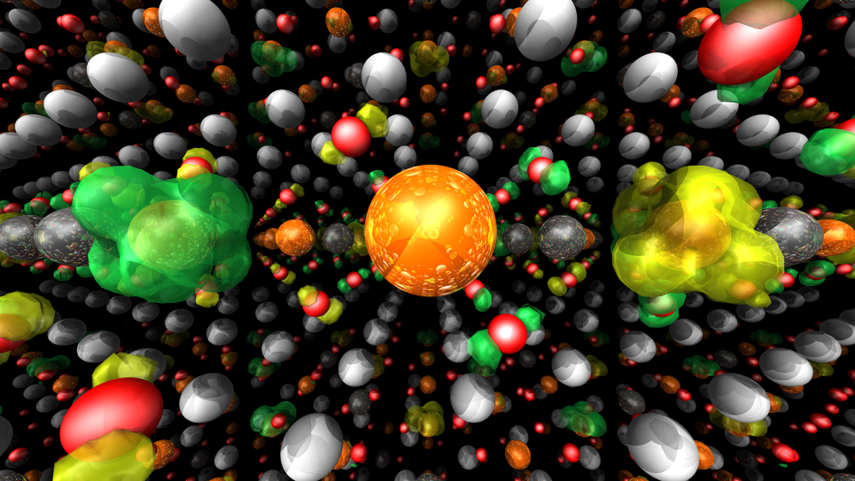
To probe the energetics governing ripple formation in these strained materials, the team performed simulations using Mira, the 10-petaflops supercomputer at the Argonne Leadership Computing Facility (ALCF), a U.S. Department of Energy Office of Science User Facility. The simulations were in excellent agreement with their experimental findings.
“We utilized a model system comprised of nearly 150,000 atoms to explore the flat-rippled conformational space,” said Robert A. DiStasio Jr., Assistant Professor in the Department of Chemistry and Chemical Biology at Cornell University and one of the paper’s lead authors. “The computational resources provided by the ALCF enabled us to perform the large-scale calculations required to validate this discovery.”
The researchers tested the material’s performance in one of the most widely used electronic devices: a diode. Two different kinds of material are joined, and electrons are supposed to be able to flow one way through the “fabric,” but not the other
The diode lit up. “It was exciting to see these three-atom-thick LEDs glowing. We saw excellent performance—the best known for these types of materials,” said Saien Xie, a graduate student and first author on the paper.
The discovery opens up some interesting ideas for electronics. Devices like LEDs are currently stacked in layers—3D versus 2D, and are usually on a rigid surface. But Park said the new technique could open up new configurations, like flexible LEDs or atoms-thick 2D circuits that work both horizontally and laterally.
He also noted that the stretching and compressing changed the optical properties—the color—of the crystals due to the quantum mechanical effects. This suggests potential for light sensors and LEDs that could be tuned to different colors, for example, or strain-sensing fabrics that change color as they’re stretched.
“This is so unknown that we don’t even know all the possibilities it holds yet,” Park said. “Even two years ago it would have been unimaginable.”
This work was carried out in collaboration with co-lead author David A. Muller at Cornell University. Other coauthors included University of Chicago postdoctoral scholars Kibum Kang and Chibeom Park and graduate student Preeti Poddar, as well as Cornell University postdoctoral scholar Ka Un Lao and graduate students Lijie Tu, Yimo Han, and Lujie Huang
The study received support from the Cornell Center for Materials Research and the Platform for the Accelerated Realization, Analysis and Discovery of Interface Materials at Cornell, the U.S. Air Force Office of Scientific Research, the National Science Foundation, and the Samsung Advanced Institute of Technology.
ALCF computing time and resources were awarded through the ASCR Leadership Computing Challenge (ALCC). The team also used computing resources at the National Energy Research Scientific Computing Center at Lawrence Berkeley National Laboratory.
Argonne National Laboratory seeks solutions to pressing national problems in science and technology. The nation's first national laboratory, Argonne conducts leading-edge basic and applied scientific research in virtually every scientific discipline. Argonne researchers work closely with researchers from hundreds of companies, universities, and federal, state and municipal agencies to help them solve their specific problems, advance America's scientific leadership and prepare the nation for a better future. With employees from more than 60 nations, Argonne is managed by UChicago Argonne, LLC for the U.S. Department of Energy's Office of Science.
The U.S. Department of Energy's Office of Science is the single largest supporter of basic research in the physical sciences in the United States and is working to address some of the most pressing challenges of our time. For more information, visit the Office of Science website.
Domains
Allocations